Back in time, during my studies, I replaced the level I ROM with 3x 2732, holding the level II ROM content.
Unfortunately one pin of that hardware extention broke off and my oldtimer stopped working.
Today I also wanted to switch to the latest ROM version 1.3
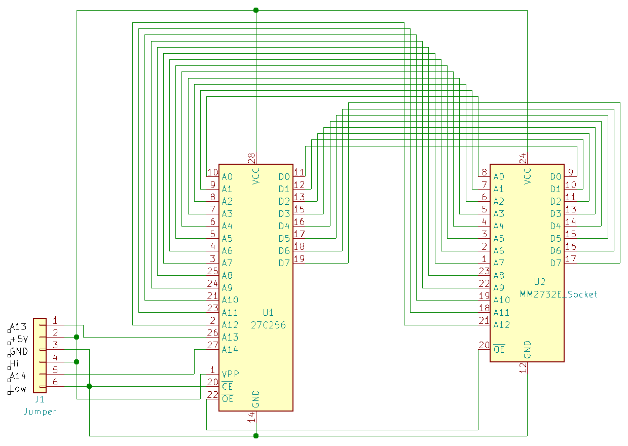
As 2732 EPROMs are no longer manufactured, it was obvious to switch to a modern 27C256 EPROM.
Further on I describe all changes in detail.
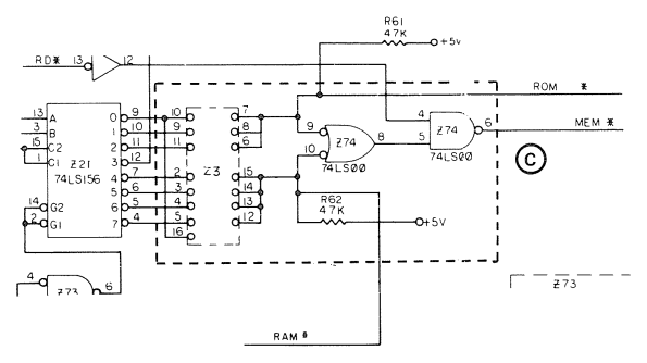
Let's start with the fundamental things. The ROM socket on my board revision D offers the address lines A0-A12,
the data lines D0-D7 and the inverted output enable (!OE) signal. That's a lot.
But a 27C256 has the address lines A13 & A14 too. A13 is required for the last 4K of ROM and with A14 one can
select between two ROM versions. For that A14 will be set by a jumper to put A14 to 0V or 5V to select the lower
or the upper part of the EPROM. With !OE the first 12K will be used anyway.
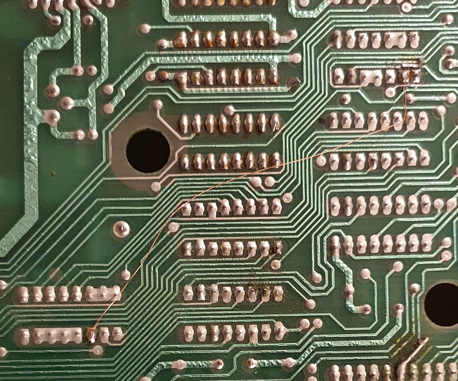
But where do I get A13? My first try, to take it from the address bus directly, tied up the whole computer.
Where do I get a buffered A13, a decoupled signal?
The solution is Z21. The address decoder devides A12 (A) and A13 (B) to four outputs. At Z21 pin 11 the inverted A13
is available.
With diodes I decoupled the outputs 9 and 10 to get the inverted A13 alone.
R61 pulls the input of Z74 to high level. The open collector outputs of Z21 delivers low signal only. This is not
disturbed by the diodes.
Thanks to Larry for his detailed observation of my instruction.
The address decoder is Z21 and not Z31. I changed the text according to that.
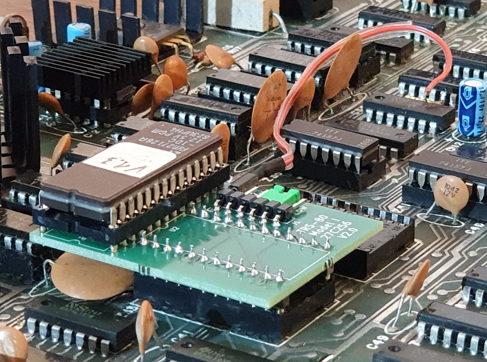
The schematic and the picture are showing Z3. Pin 1 is in the upper left corner of the picture.
The diodes are standard 1N4148.
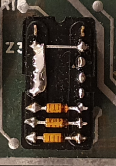
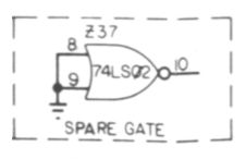
The IC Z37 is having a spare inverter. I disconnected pin 8 and pin 9 carefully. Pin 8 stays at ground level.
As Z21 pin 11 is an open collector output, pin 9 gets a 4k7 pullup resistor. Now pin 10 is offering the orginal
A13 signal.
Thanks to Larry for his hint.
If you left click on the picture and drawing, you get a larger version of it.
After that I created a PCB which connects the socket signals to the 27C256. Additional it receives the address lines
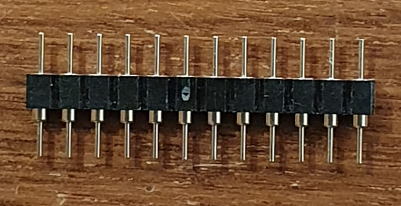
A13 and A14 via a plug connector.
I use such a plug connector to pick the signals from the socket.
If someone is interested, one can get the PCB files as Gerber format.
When you start thinking about the EPROM size, two other sizes, with the same number of pins, get into view:
27C128 and 27C512
I had a 27C128 with the only difference at pin 27. If I set A14 to 5V, with the jumper, I can use the same PCB
with my 27C128 and that is what I am doing.